Capacitors · Volume 6
Ceramic Capacitors: Class I, Class II, and What X7R Actually Means
6.1 The most common component nobody understands
A modern smartphone contains something on the order of a thousand ceramic capacitors. A laptop motherboard carries hundreds. They are the little tan, brown, or bluish blocks soldered in clusters around every power pin, and they are, by unit count, the most-manufactured discrete electronic component in history — trillions a year. They are cheap enough to be sold by the reel and priced by the thousand, small enough that the smallest are hard to pick up without tweezers and a steady hand, and reliable enough that most of them will outlive the products they go into.
They are also, for a component this ubiquitous, remarkably badly understood. A great many otherwise competent engineers believe that a capacitor marked “10 µF” is a 10 µF capacitor. For a certain very common and very useful family of ceramics, that belief is simply false — the part may deliver three or four microfarads once it is soldered into a real circuit with real voltage across it, and that is not a defect but the datasheet behaving exactly as written. The gap between the number printed on the part and the capacitance the circuit actually sees is the single most important thing an engineer can know about ceramic capacitors, and it is the reason this volume exists.
The previous volume in this series is the decoder ring: it teaches how to read the markings on a capacitor, including the compact codes stamped on ceramics. This volume is about what those codes mean — not “X7R is spelled ex-seven-arr” but “X7R is a barium-titanate dielectric that will hold its value within fifteen percent over temperature, sing faintly when you drive it with a switching waveform, quietly lose capacitance as it ages, and shed more than half its capacitance when you bias it near its rated voltage.” Reading the code is arithmetic. Understanding it is engineering.
6.2 What a ceramic capacitor is
Every capacitor is two conductors separated by an insulator, and its capacitance grows with the area of the conductors, shrinks with the distance between them, and scales with a property of the insulator called its permittivity — how strongly the material polarizes, and therefore stores energy, in an electric field. (The physics of permittivity, the equivalent circuit, and impedance-versus-frequency are the subject of the “real capacitor” volume; this one takes them as given.) A ceramic capacitor is the family whose insulator — the dielectric — is a fired ceramic: a metal-oxide powder pressed and sintered into a hard, glassy, temperature-stable, chemically inert solid.
Two families of ceramic dominate, and the difference between them is the whole story. The first is built around titanium dioxide and related paraelectric oxides — magnesium titanate, calcium zirconate, neodymium and lanthanum titanates, blended to hit a target. These have modest permittivity (a relative permittivity, εr, in the low tens up to around a hundred) but they are exquisitely stable: their permittivity barely moves with temperature, voltage, or age. The second is built around barium titanate, BaTiO₃, a ferroelectric ceramic with an enormous permittivity — εr from a couple of thousand up to eighteen thousand or more — that comes bundled with every misbehaviour a ferroelectric can offer. That single choice, paraelectric titanate versus ferroelectric barium titanate, splits the entire ceramic-capacitor world into the two “classes” this volume is built around.
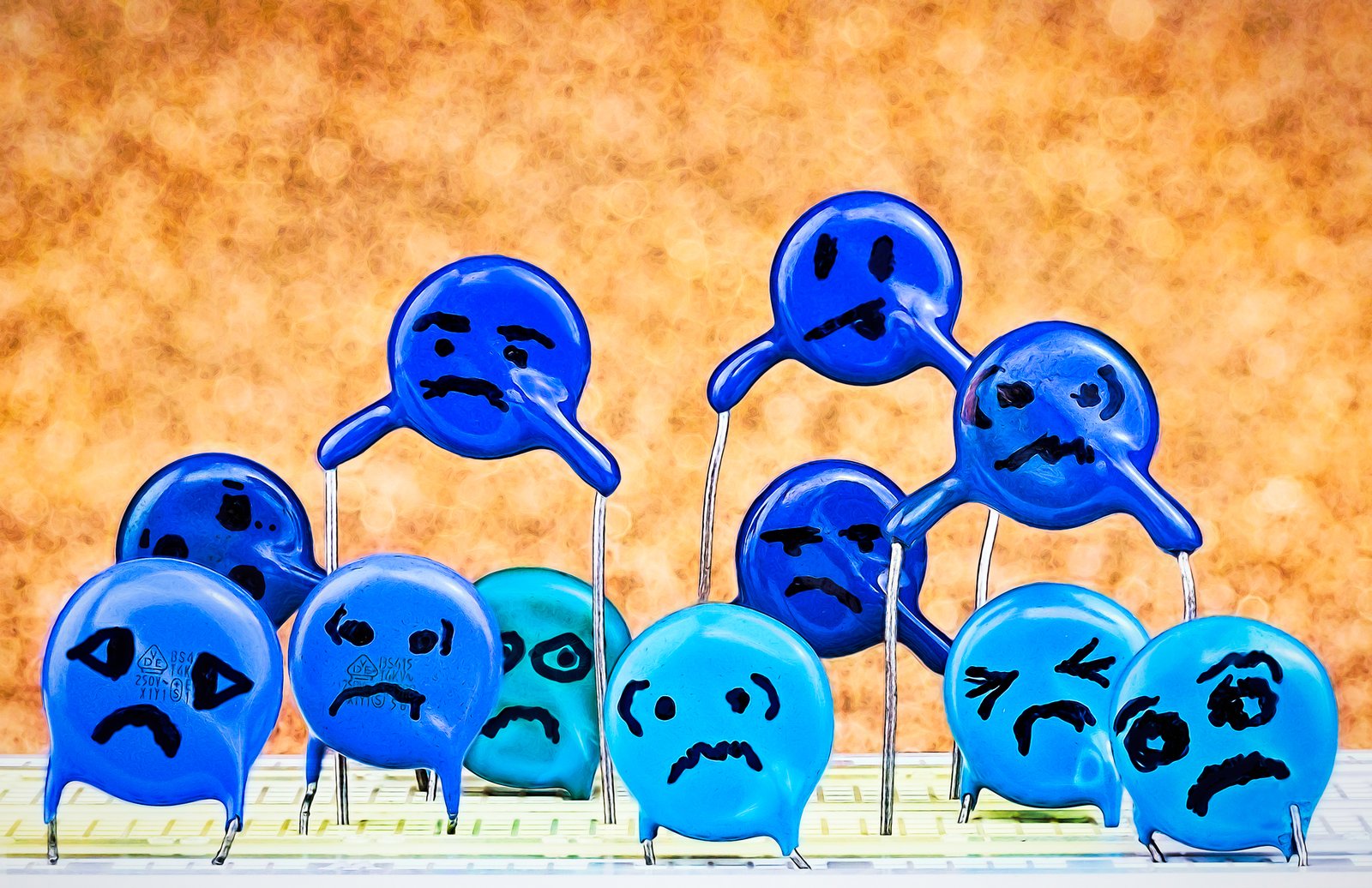
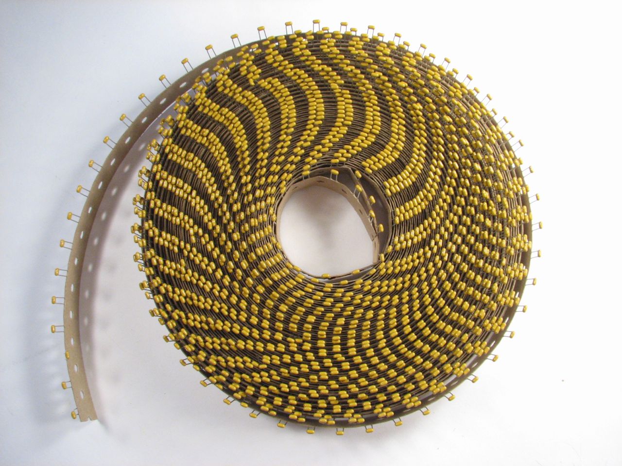
Physically the parts come in two constructions. The older is the disc (or, in tubular form, the leaded ceramic): a single wafer of ceramic with a metal electrode fired onto each face and two wires attached, dipped in epoxy or phenolic. Discs are simple, cheap, good at high voltage because the ceramic can be made thick, and they are what “ceramic capacitor” meant for most of the twentieth century — the blue and brown lentils of Figure 1. The dominant modern construction is the multilayer ceramic chip capacitor, universally abbreviated MLCC: instead of one ceramic layer, dozens to many hundreds of very thin ceramic layers are interleaved with printed metal electrodes, like a deck of cards where alternate cards connect to opposite ends, and the whole stack is co-fired into a single monolithic block with a metal termination baked onto each end.
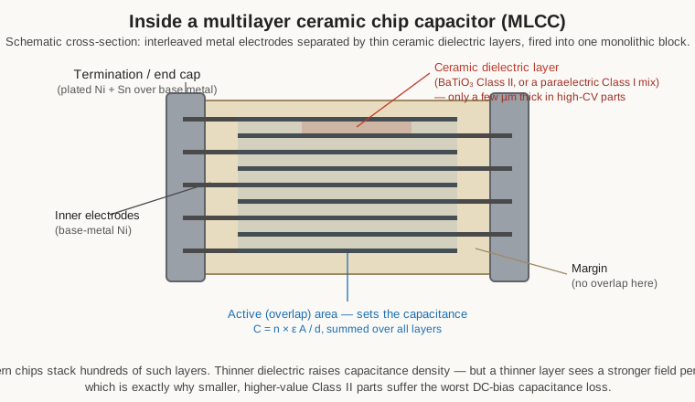
The MLCC’s stacked geometry is what makes it so formidable. Capacitance is proportional to electrode area and inversely proportional to dielectric thickness, so stacking n thin layers multiplies the capacitance roughly n-fold while keeping the part tiny. Drive the layer count up and the layer thickness down — modern high-value parts use dielectric layers only a couple of micrometres thick — and a chip the size of a grain of rice can reach tens of microfarads. The manufacturing that achieves this (tape casting, screen-printed electrodes, co-firing base-metal nickel electrodes in a reducing atmosphere) is the subject of the “how capacitors are made” volume. What matters here is the consequence: the same physics that packs so much capacitance into so little space is exactly the physics that makes high-value ceramics misbehave. Thin, high-permittivity layers are what give you the microfarads, and thin, high-permittivity ferroelectric layers are what collapse under DC bias, drift with temperature, age, and sing.
6.2.1 Why ceramics dominate
Given the misbehaviours to come, it is worth being clear about why ceramics won anyway. They are non-polarized — no plus and minus end, unlike electrolytics and tantalums, so they can never be inserted backwards and never care about the polarity of a signal. They span an enormous range, from fractions of a picofarad to hundreds of microfarads, in one technology. They are physically tiny and cheap to make in the billions. Crucially for high-frequency work, an MLCC’s stacked, short-path construction gives it very low parasitic inductance (ESL) and very low equivalent series resistance (ESR), which means low impedance and a high self-resonant frequency — the properties that make them the default choice for decoupling fast digital chips. And the ceramic itself is mechanically hard, non-flammable, and indifferent to humidity and time in a way that paper and electrolyte never are. For everything from a picofarad of RF tuning to a bulk reservoir on a 1.8 V rail, some ceramic will do the job. The engineering is in choosing which ceramic.
6.3 The class system, and the trade nobody escapes
The Electronic Industries Alliance (EIA), in standard RS-198, sorts ceramic dielectrics into classes, and the classes are really a sorting by that first design choice — paraelectric versus ferroelectric — and its consequences.
Class I dielectrics are the paraelectric, low-permittivity, temperature-compensating ceramics. Their defining virtue is predictability: capacitance changes with temperature by a small, precisely specified, nearly linear amount, and it does not meaningfully change with applied voltage, signal level, or age. They have very low dielectric loss. The price is low permittivity, which means low capacitance for a given size — a Class I part is bulky for its value. C0G (equivalently NP0) is the flagship.
Class II dielectrics are the ferroelectric, high-permittivity, temperature-stable ceramics, based on barium titanate tuned with additives. They pack far more capacitance into the same space, and they hold their value “stably enough” for general-purpose work — X7R keeps within ±15 % across a wide temperature band. The price is every ferroelectric vice: DC-bias loss, larger temperature swings, aging, voltage and frequency dependence, higher loss, and piezoelectricity. X7R, X5R, and their kin live here.
Class III dielectrics push permittivity even higher, often with a barrier-layer or reduced-titanate structure, and accept correspondingly worse stability. Y5V and Z5U are the familiar names. These deliver the most capacitance per dollar and per cubic millimetre of any ceramic, and the least trustworthy value: a Y5V part can lose more than eighty percent of its capacitance at the edges of its rated temperature range before any bias is applied. In much modern literature Class II and Class III are lumped together as “Class II” because they share the same code format and the same fundamental physics; this volume keeps the distinction where it matters and treats Y5V/Z5U as the worst-behaved members of the high-permittivity camp.
The trade underneath all three is unavoidable and worth stating plainly: permittivity and stability are in opposition. The mechanism that gives barium titanate its colossal permittivity — the alignment of ferroelectric domains, tiny regions of the crystal whose spontaneous polarization can be nudged by an applied field — is exactly the mechanism that makes that permittivity depend on temperature (the domains freeze and shift), on voltage (a strong field saturates them so they can no longer respond to signal), on time (they gradually settle into lower-energy configurations — aging), and on mechanical stress (they are piezoelectric). A paraelectric ceramic has no such domains, so it is stable — and, for the same reason, has nothing like the permittivity. You can have a lot of capacitance in a small package, or you can have a capacitance you can trust, but no single ceramic gives you both. Everything that follows is a consequence of that sentence.
6.4 Class I: C0G/NP0 and the temperature-compensating codes
C0G is the capacitor an engineer reaches for when the value must be right. Over the full −55 °C to +125 °C range its capacitance drifts by about ±0.3 % — a tempco of 0 ± 30 parts per million per degree Celsius. It shows negligible change with applied DC voltage, negligible aging, and a dissipation factor below about 0.1 % (often far below). That combination — stable, low-loss, predictable — makes it the ceramic for timing circuits, oscillator tanks, PLL loop filters, precision analog, sample-and-hold, and any RF resonator where a few parts per million of drift shifts a frequency you care about. Its only real weakness is capacitance density: because the paraelectric dielectric has εr in the tens rather than the thousands, a C0G part is much larger than a Class II part of the same value and voltage, and above roughly a microfarad the size and cost become impractical.
The name repays a moment’s attention. NP0 is the older, physically descriptive designation: Negative-Positive-zero, meaning the temperature coefficient is neither meaningfully negative nor positive but nominally zero. C0G is the EIA code for the same characteristic — and, usefully, it is not a special case but the zero-tempco member of a general, systematic code that describes any Class I temperature coefficient. That is the code the previous volume showed how to read; here is what it means.
A Class I EIA code is three characters. The first (a letter) gives the significant figures of the temperature coefficient in ppm/°C. The second (a digit) is a multiplier — a power of ten, and, importantly, a sign. The third (a letter) is the tolerance of that temperature coefficient, in ppm/°C.
Table 1 — Class I: C0G/NP0 and the temperature-compensating codes
| 1st char — significant figures (ppm/°C) | 2nd char — multiplier | 3rd char — tolerance (ppm/°C) | |||
|---|---|---|---|---|---|
| C = 0.0 | R = 2.2 | 0 = ×(−1) | 5 = ×(+1) | G = ±30 | L = ±500 |
| B = 0.3 | S = 3.3 | 1 = ×(−10) | 6 = ×(+10) | H = ±60 | M = ±1000 |
| L = 0.8 | T = 4.7 | 2 = ×(−100) | 7 = ×(+100) | J = ±120 | N = ±2500 |
| A = 0.9 | V = 5.6 | 3 = ×(−1000) | 8 = ×(+1000) | K = ±250 | |
| M = 1.0 | U = 7.5 | ||||
| P = 1.5 |
Work C0G through it: C = 0.0 significant figures, 0 = multiplier ×(−1), so the tempco is 0.0 × (−1) = 0 ppm/°C; G = ±30 ppm/°C tolerance. Zero drift, held to thirty parts per million per degree. That is the definitive answer to “what does C0G mean,” and it is why the part is trusted.
Class I is not only about zero drift, though. Because the code can express any coefficient, the family includes a ladder of deliberately non-zero, negative-tempco ceramics whose entire purpose is temperature compensation — cancelling the drift of other parts. In a classic LC oscillator the inductor and the surrounding components drift positive with temperature; dropping in a capacitor with an equal-and-opposite negative tempco holds the resonant frequency steady. These parts are named in a plain, physical shorthand rather than the terse EIA triplet: P for a positive coefficient, N for negative, followed by the magnitude in ppm/°C. P100 is +100 ppm/°C; N750 is −750 ppm/°C; the ladder runs on through N1500, N2200, and beyond to N4700. Each maps onto the systematic EIA code and an older IEC designation:
Table 2 — Class I is not only about zero drift, though. Because the code can express any coefficient, the family includes a ladder of deliberately non-zero, negative-tempco ceramics whose entire purpose is temperature compensation — cancelling the drift of other parts. In a classic LC oscillator the inductor and the surrounding components drift positive with temperature; dropping in a capacitor with an equal-and-opposite negative tempco holds the resonant frequency steady. These parts are named in a plain, physical shorthand rather than the terse EIA triplet: P for a positive coefficient, N for negative, followed by the magnitude in ppm/°C. P100 is +100 ppm/°C; N750 is −750 ppm/°C; the ladder runs on through N1500, N2200, and beyond to N4700. Each maps onto the systematic EIA code and an older IEC designation
| Industrial name | Tempco (ppm/°C) | Tolerance | EIA code |
|---|---|---|---|
| P100 | +100 | ±30 | M7G |
| NP0 / C0G | 0 | ±30 | C0G |
| N075 | −75 | ±30 | U1G |
| N150 | −150 | ±60 | P2H |
| N220 | −220 | ±60 | R2H |
| N330 | −330 | ±60 | S2H |
| N470 | −470 | ±60 | T2H |
| N750 | −750 | ±120 | U2J |
| N1500 | −1500 | ±250 | P3K |
Check N750 against the code table: U = 7.5, 2 = ×(−100) → 7.5 × (−100) = −750 ppm/°C, J = ±120. The system is entirely self-consistent once the three columns are in front of you. (Older military ceramic specifications — MIL-PRF-20 and its descendants — carry their own “characteristic” letters for these same temperature coefficients, and it is from that lineage that “NP0” comes; the EIA C0G notation has largely displaced it in commercial catalogs, but both appear on real parts and mean the same thing.)
6.5 Class II and III: the codes, decoded
Where a Class I code describes a slope, a Class II/III code describes a box: the temperature range over which the part is characterized, and how far the capacitance is allowed to wander inside it. The three characters are read completely differently from the Class I triplet — a trap for the unwary, because both are three-character codes stamped on ceramic capacitors.
The first character (a letter) is the low-temperature limit. The second character (a digit) is the high-temperature limit. The third character (a letter) is the maximum capacitance change over that whole range, expressed as a percentage relative to the value at 25 °C (measured at low signal, with no DC bias — a caveat that will matter enormously in a moment).
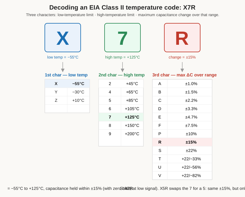
Table 3 — Class II and III: the codes, decoded
| 1st char — low-temp limit | 2nd char — high-temp limit | 3rd char — max ΔC over range |
|---|---|---|
| X = −55 °C | 2 = +45 °C | A = ±1.0 % · B = ±1.5 % · C = ±2.2 % |
| Y = −30 °C | 4 = +65 °C | D = ±3.3 % · E = ±4.7 % · F = ±7.5 % |
| Z = +10 °C | 5 = +85 °C | P = ±10 % · R = ±15 % · S = ±22 % |
| 6 = +105 °C | T = +22/−33 % | |
| 7 = +125 °C | U = +22/−56 % | |
| 8 = +150 °C | V = +22/−82 % | |
| 9 = +200 °C |
Now the common names decode themselves:
- X7R — X (−55 °C), 7 (+125 °C), R (±15 %). The general-purpose workhorse: usable to automotive-under-hood temperatures, value held within ±15 % across the whole span. The most-specified Class II dielectric there is.
- X5R — X (−55 °C), 5 (+85 °C), R (±15 %). Same ±15 % stability, but rated only to +85 °C. Trading the top of the temperature range buys thinner dielectric formulations and therefore more capacitance in a given case size, which is why bulk decoupling on low-voltage rails is so often X5R rather than X7R.
- X8R / X8L — X (−55 °C), 8 (+150 °C). High-temperature Class II for automotive and industrial work; the L third-character variants relax the tolerance at the very top of the range.
- Y5V — Y (−30 °C), 5 (+85 °C), V (+22 %/−82 %). A Class III barrier-layer dielectric: maximum capacitance per unit cost, and a value that can fall to under a fifth of nominal at the ends of its range. Only −30 °C at the cold end, too.
- Z5U — Z (+10 °C), 5 (+85 °C), U (+22 %/−56 %). The other classic Class III part: note the cold limit of only +10 °C, which alone disqualifies it from anything that has to work outdoors in winter.
The letter tolerances in the third column are worth internalizing because the good ones and the terrible ones sit in the same code. R (±15 %) and F (±7.5 %) describe a part you can loosely design around. V (+22 %/−82 %) describes a part whose capacitance is a suggestion. Two capacitors can look identically cryptic on the reel — “X7R” and “Y5V” are the same length and the same alphabet soup — and be an order of magnitude apart in trustworthiness. This is the single most useful thing to carry away from the code: the third letter is the character reference, and V means “do not rely on me.”
6.6 The four ways Class II ceramics misbehave
Every Class II and Class III part carries the code’s promise and four unwritten warnings. An engineer who knows only the code will be surprised on the bench; an engineer who knows the four warnings will not. Class I ceramics are, usefully, largely immune to all four — a point worth remembering when one of them decides the answer.
6.6.1 DC bias: the killer effect
This is the one that catches everyone, and it is the reason the “10 µF ceramic” on a power rail may be three microfarads in circuit. A ferroelectric dielectric’s high permittivity comes from domains that reorient in response to an applied field. Put a steady DC field across the dielectric — which is exactly what happens when the capacitor sits on a DC power rail — and those domains progressively align with it and saturate. Once saturated they can no longer respond to additional field, so the incremental permittivity, which is what capacitance actually measures, falls. As the DC bias climbs toward the part’s rated voltage, capacitance collapses.
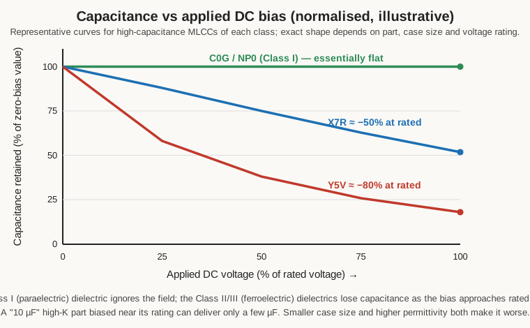
How bad is it? Bad enough to change designs. Representative manufacturer data for a small, high-capacitance-density part — a 10 µF, 6.3 V, X5R in an 0805 case — shows capacitance falling by 60 to 70 % when biased at only 3.3 to 5 V; the “10 µF” part delivers three or four microfarads at its operating point. Measurements on 10 µF 6.3 V X7R parts from various vendors cluster in the −35 % to −65 % range at rated voltage, and — a nasty subtlety — two parts with identical markings from different manufacturers can have markedly different bias curves, so a second-source substitution that matches value, voltage, and dielectric on paper can still change the delivered capacitance. C0G, by contrast, is essentially flat: a paraelectric dielectric has no domains to saturate, so its capacitance ignores the bias.
Three variables make DC-bias loss worse, and all three point the same way as the capacitance-density race. Smaller case size is worse, because squeezing a given value into a smaller chip demands thinner dielectric layers, and a thinner layer sees a stronger field (volts per micrometre) for the same applied voltage. Higher permittivity is worse, because the more ferroelectric the dielectric, the more there is to saturate — so a Y5V droops far more steeply than an X7R, which droops more than a C0G. And operating closer to the rated voltage is worse, obviously, since that is the axis of the curve. The mitigations follow directly: derate the voltage generously (a common rule of thumb is to pick a voltage rating two to three times the working voltage, so a 3.3 V rail gets 10 V or 16 V parts, not 4 V or 6.3 V ones); over-specify the capacitance so that even the biased value meets the requirement; move up a case size to get thicker layers; or, where the delivered value genuinely must be known — a timing network, a filter corner — use Class I and pay the size penalty. Manufacturers publish the bias curves, and tools such as Murata’s SimSurfing plot them per part; consulting that curve before finalizing a high-K MLCC is the difference between a bulk capacitor and a decorative one.
6.6.2 Temperature: the ±15 % that isn’t a rounding error
The temperature behaviour is the one the code openly advertises, so it should never be a surprise — yet the magnitude still catches people who read “X7R” as “stable.” X7R’s ±15 % means a nominal 100 nF part is guaranteed only to be somewhere between 85 nF and 115 nF across its range, and that is the good Class II dielectric. Y5V’s +22/−82 % means the same nominal value is allowed to sit anywhere from 122 % down to 18 % of nominal — a better-than-five-to-one span — with the deep loss concentrated at the hot and cold extremes.
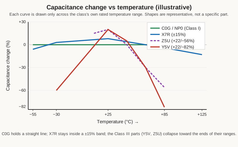
The shapes matter as much as the limits. A C0G traces a nearly flat, gently sloped line — that is the whole point of it. An X7R stays inside its ±15 % band but is not flat within it, typically bulging slightly positive near room temperature and falling toward the band edges at the extremes. Y5V and Z5U look stable only in a narrow window around room temperature and then dive; a Z5U that reads on-value on the bench at 25 °C may have lost half its capacitance by the time the equipment reaches 85 °C. And this is the bias-free temperature behaviour — the DC-bias loss of the previous section stacks on top of it, so a high-K part that is warm and biased near rated voltage can be a long way below its label on both counts at once.
6.6.3 Aging: the capacitor that quietly shrinks
This one is invisible unless you know to look for it, and it applies to Class II and III only. Barium titanate is ferroelectric below its Curie temperature — the transition point, around 120–130 °C, above which the crystal loses its spontaneous polarization. When a freshly fired MLCC cools through the Curie point, its ferroelectric domains are in a high-energy, disordered state, and over time they relax toward lower-energy configurations. The macroscopic consequence is that capacitance decreases logarithmically with time after firing — fast at first, then ever more slowly, losing a roughly constant percentage per decade of elapsed time (per decade-hour: the loss from 1 to 10 hours equals the loss from 10 to 100 hours equals the loss from 100 to 1000 hours).
The aging rate is part of the dielectric’s character. X7R ages at roughly 1–2 % per decade-hour (often quoted near 1.3 %); the higher-permittivity Class III dielectrics age faster, Z5U at something like 4–6 % per decade-hour. C0G, being paraelectric, does not age meaningfully at all. The practical upshots are two. First, when you measure matters: a part measured an hour off the production line reads higher than the same part measured a week later, so datasheet capacitance is specified at a reference age (commonly 1000 hours) and a “fresh” reading will look high. Second — and this is the elegant part — aging is fully reversible. Heat the part back above its Curie point (a de-aging bake, typically around 150 °C for an hour or so), let it cool, and the domains reset to their disordered high-capacitance state; the aging clock starts again from zero. Any reflow-soldering step does exactly this incidentally, which is why the aging clock on a board effectively resets when it is assembled. It also means a decades-old X7R measured cold can read low purely from accumulated aging, and a bake will “restore” capacitance that was never really lost.
6.6.4 Voltage/frequency coefficients and the singing capacitor
The fourth warning is really a cluster of smaller effects with a common ferroelectric root, and one of them is audible. Because the dielectric’s permittivity depends on the instantaneous field, Class II capacitance also depends on the AC signal level across it (an AC voltage coefficient, distinct from the DC-bias effect) and on frequency, and its dissipation factor is far higher than Class I’s — a few percent for X7R against under a tenth of a percent for C0G, and higher still for Y5V. None of these are catastrophic in decoupling, but they disqualify Class II from precision filtering and low-distortion audio signal paths, where the capacitance moving with the signal is literally distortion.
The showpiece of the cluster is piezoelectricity. Ferroelectric barium titanate is piezoelectric: mechanical stress produces a voltage, and — the effect that matters here — an applied voltage produces mechanical strain. A Class II MLCC physically changes shape, very slightly, with the voltage across it. Drive it with the ripple and switching edges of a switched-mode power supply and it flexes at those frequencies; if any of that spectrum lands in the audio band, the capacitor — and the board it is soldered to, which it drives like a diaphragm — emits an audible hiss, buzz, or whine. This is the notorious “singing capacitor” or “coil whine that turns out not to be the coil,” and it is a genuine, common SMPS complaint. The effect runs both ways: the same part acts as a microphone, converting board vibration and acoustic noise into electrical noise, which is why a Class II coupling capacitor in a sensitive audio or sensor front-end can inject microphonic noise. C0G and NP0, having no ferroelectric domains, are not piezoelectric and do neither — one more reason they own the precision and low-noise sockets. Mitigations for the singing include specialized low-distortion or “low-acoustic-noise” MLCC series, splitting one large capacitor into several smaller ones, orienting parts to oppose their flex, and, where it truly matters, using a film or C0G capacitor instead.
6.7 Voltage ratings, case sizes, and the density race
A ceramic capacitor is specified by capacitance, tolerance, dielectric class, and rated DC working voltage — and, as the DC-bias section made clear, that voltage rating is not merely a “do not exceed” limit but an input to how much capacitance you actually get. Common ratings run 4, 6.3, 10, 16, 25, 50, 100 V and up into the kilovolts for specialized discs; the higher the rating for a given case size and value, the thicker the dielectric and so the gentler the bias curve.
Case sizes follow the EIA imperial-footprint code, a four-digit number giving length and width in hundredths of an inch: 0201 (0.6 × 0.3 mm), 0402, 0603, 0805, 1206, 1210, on up to 1812 and 2220 — and, at the small extreme, 01005 (0.4 × 0.2 mm), a part genuinely difficult to see. Larger cases hold more capacitance and more voltage and suffer less DC-bias loss, but eat board area; smaller cases are denser and cheaper to place but bias-droop harder. The relentless trend has been toward smaller cases at higher capacitance — the “capacitance-density race” — achieved by making dielectric layers ever thinner and stacking more of them, which is precisely the recipe that makes each new generation of tiny high-value part more bias-sensitive than the last. There is no free lunch; there is only a smaller lunch that saturates sooner.
6.8 Cracking: the mechanical failure mode
The MLCC’s great weakness is not electrical but mechanical: it is a small, hard, brittle ceramic monolith rigidly soldered at both ends to a board that bends. The dominant field failure is the flex crack (board-flex crack). When the PCB flexes — during depaneling, connector insertion, mounting-screw torque, handling, or vibration — the strain concentrates at the rigid solder joints and can open a crack running diagonally up through the ceramic from a termination. The crack may sever electrodes (open or reduced capacitance) or, worse, bridge opposing electrodes through a partially conductive path, producing a low-resistance leakage or a dead short on a power rail — a failure that can smoke a board.
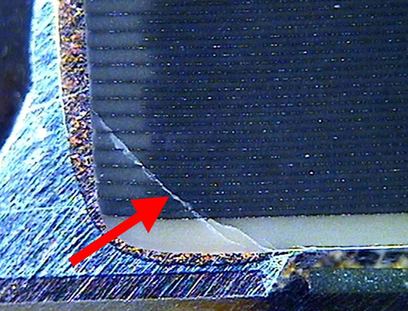
A second mechanism is thermal cracking during soldering: ceramic is a poor conductor of heat and has limited thermal-shock tolerance, so slamming a cold chip with a hot iron or an aggressive reflow ramp can crack it outright. Hand-soldering large MLCCs with a soldering iron is a classic way to induce hidden cracks that fail weeks later. The mitigations are a mix of layout and part choice: preheat and use controlled reflow ramps rather than direct iron contact on big chips; orient capacitors so their long axis lies along the direction of least board flex, and keep them away from board edges, mounting holes, connectors, and depaneling routes where strain peaks; use smaller cases (which tolerate more flex) where possible; add local slots or scoring to isolate strain-prone regions; and, for anything mechanically demanding, specify flexible (soft) termination parts, which incorporate a conductive-polymer layer in the end cap that absorbs board strain and dramatically raises the flex a part can survive before cracking. Because a cracked ceramic can fail short, safety-relevant and reliability-critical designs also consider series or fused arrangements so a single cracked chip cannot bring down a rail. Impedance, ESR, and self-resonance — the properties that decide how a healthy ceramic performs in the circuit — are treated in the “real capacitor” volume; cracking is the reminder that all of that assumes the part survived assembly intact.
6.9 Where each ceramic wins
The decision, stripped to a sentence for each: reach for C0G/NP0 when the value must be right — timing, oscillators, PLL loop filters, RF resonators, precision analog, low-distortion signal paths, anywhere drift or a voltage coefficient becomes an error you can measure; accept that it is bulky and impractical above roughly a microfarad. Reach for X7R for everyday decoupling and bypass across a wide temperature range, wherever ±15 % (before bias) is acceptable and you want a lot of capacitance in a little space; it is the sensible default for the clusters of caps around a digital chip. Reach for X5R when you need microfarads in a tiny space on a low-voltage rail and can live with only +85 °C and the same ±15 %; it is the bulk-decoupling ceramic of dense, cool, low-voltage boards. Avoid Y5V and Z5U unless the application genuinely does not care — a non-critical bulk reservoir where you simply need “a lot of cheap capacitance” and the value can wander by four or five to one over temperature, bias, and age without consequence; their cold limits (−30 °C for Y5V, +10 °C for Z5U) alone rule them out of most equipment that leaves a heated room. And across all of the Class II and III choices, remember that the number on the part is the starting value: subtract the DC bias, subtract the temperature swing, subtract the aging, and design around what is left. The engineer who does that is rarely surprised. The one who trusts the marking is the one wondering why a rail with “a hundred microfarads of ceramic” on it is sagging under load.
The application-by-application selection framework — how ceramics stack against film, electrolytic, and tantalum for decoupling, bulk, coupling, timing, filtering, and snubbing — is the subject of the selection volume; how these parts are co-fired from tape-cast ceramic and base-metal electrodes belongs to the manufacturing volume; and how to read the terse codes that this volume has spent its length interpreting is the markings volume that precedes it. What this volume has argued is narrower and, for a working engineer, more urgent: that “ceramic capacitor” names two nearly opposite components wearing similar clothes, that the class code tells you which one you are holding, and that for the high-permittivity half, the value printed on the part is the beginning of the calculation, not the end of it.
Comments (0)