Resistors · Volume 12
Where Resistors Are Used and How to Choose
12.1 The most versatile two terminals in electronics
Eleven volumes have taken the resistor apart: the physics that makes a material resist, the non-ideal part with its tolerance and tempco and noise, the history, the manufacture, the color code, the fixed families, the power limits, the networks and pots, and the sensing cousins. This volume puts the part back to work. A resistor, after all, is bought not for what it is but for what it does, and what it does is astonishingly varied for a component with only two terminals and one number. The same anonymous 10 kΩ chip that sets a logic pin’s resting state on one board fixes an amplifier’s gain on the next, damps a switching spike on a third, and holds a bias point steady on a fourth. The genius of the resistor is that a single, cheap, passive, temperature-tolerant element — nothing but controlled opposition to current — turns out to be the glue that every other component needs.
This volume is a tour of the jobs a resistor does, each with its own sizing logic and a small schematic, followed by the decision: how a designer actually chooses a resistor once the value is known — because value is only the first of eight questions, and for a surprising number of circuits it is not even the important one. The recurring lesson, echoed from earlier volumes, is that a resistor is “just a resistor” right up until precision, power, or noise is on the line — and then every one of the fourteen volumes converges on the choice.
12.2 A tour of the jobs a resistor does
12.2.1 Pull-up and pull-down: setting a default
Digital logic lives in two states, high and low, but a wire left floating is in neither — it drifts to whatever stray charge and leakage put it at, picks up noise, and reads randomly. The job of a pull-up or pull-down resistor is to give a node a definite resting state when nothing is actively driving it. A pull-up ties the node through a resistor to the positive supply, so it rests high unless something pulls it low; a pull-down ties it to ground, so it rests low unless something pulls it high. The resistor, not a hard wire, is essential: it is weak enough that an active driver can easily overpower it and force the other state, while still being strong enough to defeat leakage and noise when the node is left alone.
The classic home of the pull-up is the open-drain (or, in bipolar logic, open-collector) output. Such an output can only pull its pin down to ground; it has no transistor to drive the pin up. Left to itself it would float when not pulling low, so an external pull-up supplies the high level. This arrangement has a wonderful property: several open-drain outputs can share one wire, each able to pull it low, none able to fight the others by driving high — a wired-AND bus. The pin sits high (via the single pull-up) unless any device pulls it low. That is exactly how an interrupt line shared by many peripherals works, and it is the electrical foundation of the I²C two-wire bus, where both the clock (SCL) and data (SDA) lines are open-drain with a pull-up at one point on the bus.
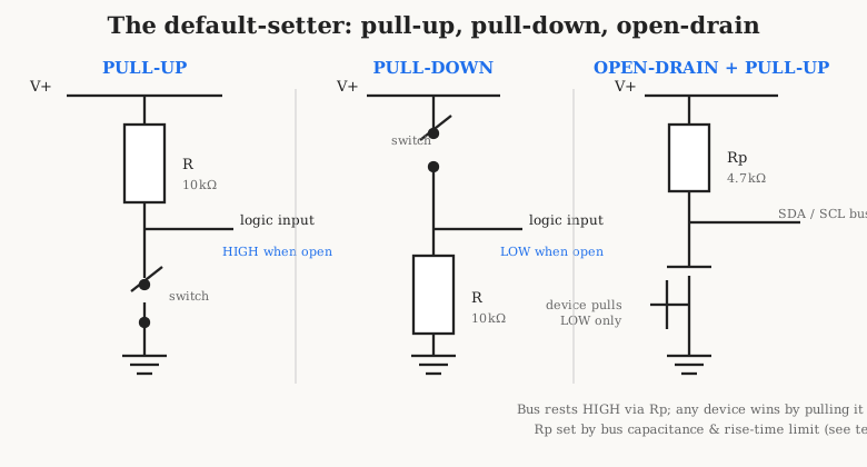
Sizing an ordinary logic pull-up or pull-down is loose: anywhere from about 1 kΩ to 100 kΩ works, with 10 kΩ the reflexive default. The trade is simple. Lower resistance means more current when the node is pulled to the opposite rail, which wastes power (a 1 kΩ pull-up to 3.3 V burns 3.3 mA whenever the node is low) but makes the node stiffer against noise and faster to snap back. Higher resistance saves power but slows the return and leaves the node more vulnerable to leakage and capacitive pickup. For a static enable pin, 100 kΩ is fine; for a noisy or fast line, 10 kΩ or less.
The I²C pull-up is the one case where the value genuinely must be calculated, because it forms an RC low-pass with the bus’s parasitic capacitance and that RC sets how fast the line can rise. When a device releases the line, nothing actively drives it high; the pull-up must charge the whole bus capacitance up through itself, and the rise time is roughly t_r ≈ 0.85 · R_p · C_bus. The I²C specification caps the bus capacitance at 400 pF and caps the rise time by speed grade: 1000 ns in standard mode (100 kHz) and 300 ns in fast mode (400 kHz). Turn the rise-time cap around and it sets the largest allowable pull-up: R_p(max) ≈ t_r / (0.85 · C_bus). At the same time the pull-up cannot be too small, because when a device pulls the line low it must sink the pull-up’s current while holding its output below the low-level threshold (typically ≤ 0.4 V), and the I²C spec limits that sink current to 3 mA — so R_p(min) ≈ (V_dd − 0.4 V) / 3 mA. A worked case: a 3.3 V fast-mode bus with 100 pF of capacitance needs R_p no larger than 300 ns / (0.85 · 100 pF) ≈ 3.5 kΩ and no smaller than (3.3 − 0.4) / 3 mA ≈ 970 Ω. The famous “4.7 kΩ” default is simply a comfortable middle value for a short standard-mode bus with a few devices (≈ 50 pF); a heavily loaded or fast bus is pulled down toward 2.2 kΩ or 1 kΩ. This is the model for how every pull-up should be reasoned about: not a magic number but a balance of rise time, sink current, and power.
12.2.2 Current limiting: fixing how much flows
The second great job is to limit current — to soak up the difference between a supply voltage and a device’s own voltage and thereby set the current at a chosen, safe level. The archetype is the series resistor that keeps an LED alive, and it recurs from Volume 1 because it is the single most-repeated calculation in electronics. An LED is stubbornly non-ohmic: below its forward voltage it barely conducts, and above it the current shoots up nearly vertically for a whisker more voltage. Wired straight across a supply it would draw destructive current in an instant. A plain series resistor tames it, because the resistor is ohmic and drops exactly the leftover voltage at the current the designer picks.
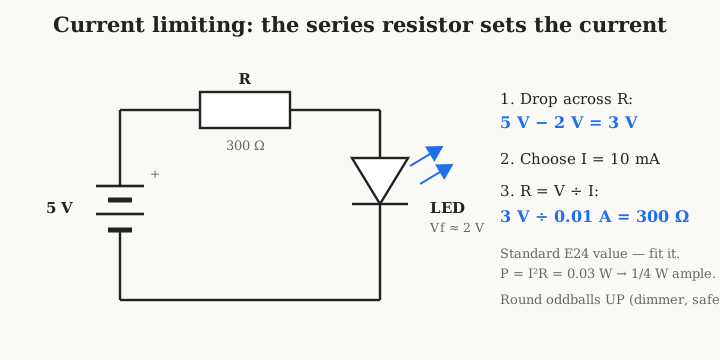
The recipe is R = (V_supply − V_f) / I. From a 5 V supply, a red LED holding V_f ≈ 2 V leaves 3 V for the resistor; for a comfortable 10 mA indicator current, R = 3 V / 0.010 A = 300 Ω, a standard value that dissipates only I²R = 0.03 W and is happy in the smallest ¼ W part. Land on an oddball number and one rounds up to the next standard value — trading a hair of brightness for a part that exists and a slightly gentler current. The same three-step ritual — find the voltage to drop, choose the current, divide for resistance, then check the power — serves anywhere a fixed current is wanted from a fixed voltage.
Current limiting wears other hats. A base resistor feeds a bipolar transistor’s base: the base-emitter junction clamps at about 0.7 V, so the resistor from the driving logic pin sets the base current, and one sizes it to deliver enough base current to saturate the transistor at the wanted collector current (base current ≈ collector current divided by the transistor’s worst-case gain, with margin). A gate resistor for a MOSFET does something subtler: a MOSFET gate draws no steady current, but it is a capacitor, and the series gate resistor limits the peak charge/discharge current from the driver and — with the gate capacitance — slows the switching edge on purpose, damping the ringing that a fast edge excites in the gate loop’s parasitic inductance. Too small a gate resistor rings and radiates; too large slows switching and raises switching loss. And an inrush limiter is a series resistor (often an NTC thermistor from Volume 11, which starts high and self-heats low, or a resistor briefly bypassed by a relay) that holds down the surge when a supply first charges a big bulk capacitor through a near short.
12.2.3 Biasing: holding a device at its operating point
Biasing is the art of using resistors to set the quiescent, no-signal operating point of an active device so that the signal has room to swing. A bipolar amplifier stage is the textbook case: a pair of resistors forms a divider that sets the base voltage, an emitter resistor sets the emitter current and stabilizes it against temperature (as the transistor warms and tries to draw more current, the emitter resistor develops more voltage and pushes back — negative feedback that a bare transistor lacks), and a collector resistor turns the collector current into an output voltage swing. None of these values is critical to a percent; what matters is that they place the collector roughly mid-supply so the output can swing both ways without clipping, and that the emitter degeneration is enough to make the bias immune to the transistor’s loose, temperature-sensitive gain.
Op-amps need bias too, but of a different kind. An ideal op-amp draws no input current; a real one draws a small input bias current, and if the two inputs see different source resistances that bias current produces different voltage drops and hence an input offset error. The classic fix is a bias-compensation resistor: make the resistance seen by the non-inverting input equal to the parallel combination of the feedback and input resistors seen by the inverting input, so the equal bias currents produce equal, cancelling drops. Here the resistor’s job is not to set a level but to match a source impedance — a foretaste of the theme that dominates precision analog design.
12.2.4 Voltage dividers and references: the ratio, and its drift
A voltage divider is the simplest and most common resistor circuit after the single series resistor: two resistors in series across a voltage, with the output taken from their junction. The output is V_out = V_in · R2 / (R1 + R2) — a fraction of the input set purely by the ratio of the two legs. Dividers scale a signal down to an ADC’s input range, set a comparator’s threshold, program a regulator’s feedback pin, and derive a reference from a higher rail.
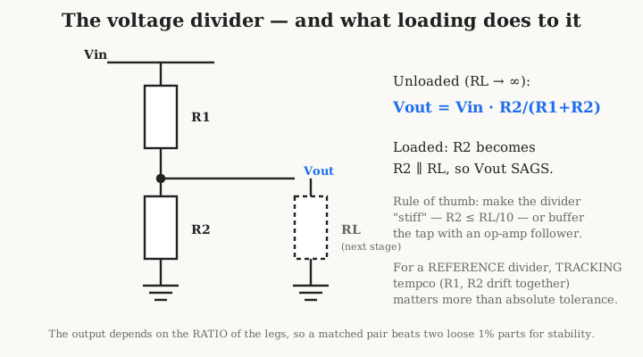
Two subtleties bite the unwary. The first is loading. The clean formula assumes nothing draws current from the tap. Connect a real load — the input resistance of the next stage — and that load appears in parallel with R2, lowering the effective lower leg and sagging the output below its predicted value. The cures are to make the divider stiff (choose R1 and R2 small enough that the load’s resistance is at least ten times R2, so it barely perturbs the ratio) or to buffer the tap with an op-amp voltage follower whose enormous input resistance draws essentially nothing. Stiff dividers waste standing current; buffered dividers cost an op-amp; the designer picks.
The second subtlety is the one that separates a casual divider from a reference divider, and it is the crux of resistor selection for precision analog work: what matters is not the absolute accuracy of R1 and R2 but how well their ratio holds — especially over temperature. Because the output depends only on the ratio R2 / (R1 + R2), two resistors that are each 1 % off but off in the same direction give a nearly perfect ratio, while two resistors each trimmed to 0.1 % absolute but drifting apart with temperature give a ratio that wanders. If R1 and R2 have independent temperature coefficients of 100 ppm/°C, their ratio can drift by up to 200 ppm/°C — 0.02 % per degree, catastrophic for a reference. If instead they are a matched pair on one chip (Volume 10) whose tempcos track to within a few ppm/°C, the ratio holds even as both legs drift together, because the drift cancels in the ratio. This is why a reference divider is built from a thin-film network or a matched pair, and why paying for 0.1 % absolute tolerance while ignoring tracking tempco is one of the most common — and most expensive — mistakes in the field.
12.2.5 Feedback and gain-setting: the ratio is the whole thing
The point sharpens in an amplifier’s feedback network, where resistors set gain. A non-inverting op-amp stage has a gain of A_v = 1 + R_f / R_g; an inverting stage has A_v = −R_f / R_in. In both, the gain is a ratio of two resistors, and — this is the load-bearing insight — a precise ratio does not require precise absolute values.
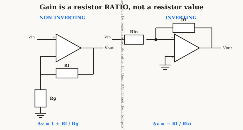
Consider a stage meant for a gain of exactly 10, built as R_f = 9 kΩ and R_g = 1 kΩ (A_v = 1 + 9 = 10). If both resistors are made 5 % high, the gain is 1 + (9.45 / 1.05) = 1 + 9 = 10 — unchanged, because the error cancels in the ratio. What sets the gain error is only the mismatch between R_f and R_g, and what sets the gain drift is only the difference in their tempcos. Two resistors from the same reel might match to a percent or two and track to a few tens of ppm/°C; two elements of a thin-film network match to 0.1 % or better and track to under 5 ppm/°C. So the precision engineer setting a gain does not reach for two individually super-accurate 0.01 % parts — that spends money on the wrong axis — but for a matched network whose relative accuracy and tracking are tight even if its absolute value is only 1 %. The same logic governs the four resistors of a difference or instrumentation amplifier, whose common-mode rejection is limited entirely by ratio mismatch: a 0.1 % mismatch caps CMRR near 66 dB, while a laser-trimmed matched network pushes it far higher. Absolute tolerance buys nothing here; matching and tracking buy everything.
12.2.6 Terminations: matching the line so it does not ring
At high speed a wire stops behaving like a simple connection and becomes a transmission line with a characteristic impedance Z₀ — the ratio of voltage to current for a wave travelling along it, set by the geometry (trace width, dielectric, spacing), not by length. A fast edge launched into such a line travels as a wave, and when that wave reaches a point where the impedance changes — an unterminated end, a mismatched load — part of it reflects back, exactly as a rope-wave bounces off a fixed end. The reflection coefficient is Γ = (R − Z₀) / (R + Z₀); the reflected energy shows up as ringing, overshoot, undershoot, and false edges that corrupt data. The cure is a termination resistor equal to Z₀, which absorbs the incoming wave completely (Γ = 0), as if the line simply continued forever.
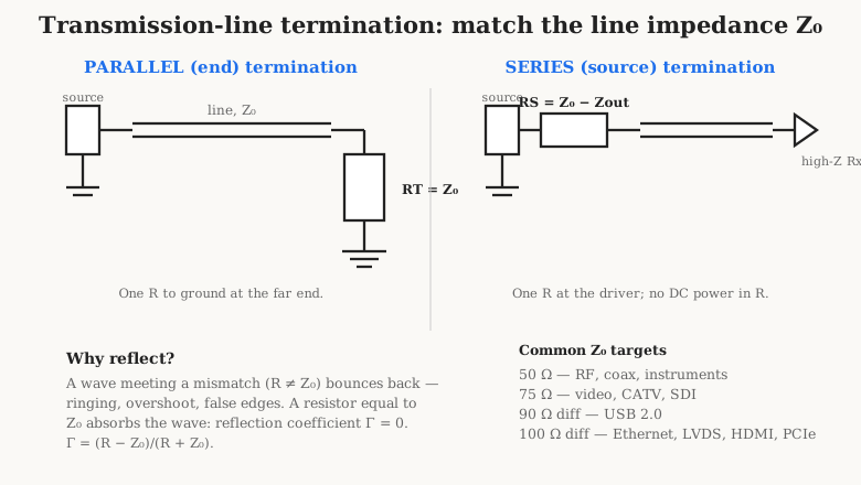
The standard impedances are worth memorizing because they dictate the termination values a designer stocks. 50 Ω is the universal RF, coaxial, and instrumentation impedance; 75 Ω is video, CATV, and SDI; and for the differential pairs of modern digital buses, 90 Ω is USB 2.0, while 100 Ω differential covers Ethernet, LVDS, HDMI, DisplayPort, and PCIe. There are several ways to place the terminating resistor. Parallel (end) termination puts a single resistor equal to Z₀ from the far end of the line to ground (or to a mid-rail via a Thévenin pair of two resistors, which also sets a DC bias); it is simple and absorbs reflections well but burns steady DC current. Series (source) termination puts a resistor at the driver equal to Z₀ minus the driver’s own output impedance, so the driver plus resistor together match the line; it draws no DC current (the far end is high-impedance) and suits point-to-point CMOS links, at the cost of only working for a single receiver at the end. AC termination puts a resistor in series with a small capacitor to ground, matching at high frequency while blocking DC to save power. The choice among them is a power-versus-topology trade, but the resistor value itself is not negotiable: it must equal the line’s Z₀, and it must hold that value at the frequencies of interest — which is why terminations favour small, low-inductance thin-film or thick-film chips placed hard against the receiver, not wirewound parts whose inductance would itself reflect.
12.2.7 RC filters, timing, snubbers, bleeders, and ballast
Pair a resistor with a capacitor (Volume on Capacitors) and the resistor’s job becomes setting a time. The product τ = R · C is the time constant that governs how fast the capacitor charges or discharges through the resistor, and it is the heart of the RC low-pass filter, whose cutoff frequency is f_c = 1 / (2π R C) — above it, signals are rolled off. The resistor sets the corner with the capacitor, and it also sets the filter’s source impedance and damps the node. The same τ times an oscillator or a one-shot to set a period, debounces a switch, or slews a control voltage gently.
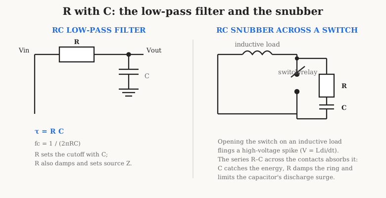
Three power-side jobs round out the tour. A snubber is an RC network placed across a switch, a relay contact, a triac, or a diode to damp the transient that switching an inductive load produces. Interrupt the current in an inductor and it answers with V = L · di/dt — a spike that can arc a relay contact or punch through a semiconductor; the series R–C across the switch gives that energy somewhere to go, the capacitor absorbing the spike and the resistor damping the resulting oscillation and limiting the surge when the capacitor later discharges. A bleeder resistor sits permanently across a power supply’s bulk capacitor so that when the supply is switched off the stored charge drains away safely in a few time constants instead of lurking at lethal voltage for hours — a safety part sized to bleed the capacitor down within a specified time while wasting acceptably little standing power in normal operation. And ballast or current-sharing resistors are small values placed in series with each of several devices run in parallel — paralleled power transistors, LEDs, or battery cells — so that the device that tries to hog the current develops more voltage across its ballast resistor and is pushed back toward its share, forcing the load to divide evenly despite the devices’ mismatched characteristics. In every one of these the resistor is doing what it always does — turning current into a proportional voltage — but in service of timing, damping, safety, or sharing rather than a signal.
12.3 The decision: how to actually choose a resistor
With the jobs surveyed, the practical question is how a designer moves from “I need about 4.7 kΩ here” to a specific part number. The value is only the first of eight considerations, and — as the tour kept showing — often not the decisive one. What follows is an ordered checklist; the order matters, because each step can override the defaults of the ones before it.
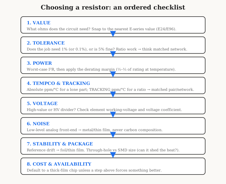
1 — Value. Start with the ohms the circuit needs, then snap to the nearest value the world actually makes: an E-series value (Volume 6). General parts come in E24 (5 %); precision parts in E96 (1 %) or E192 (0.1 %). If the exact value matters — a divider ratio, a filter corner — pick the E96 value that lands closest, or synthesize it from a series/parallel pair, or use a value that the ratio makes exact even if neither leg is round. Design in standard values from the start; an “ideal” 3.9 kΩ that has to become 4.7 kΩ at the shelf is better discovered on paper than at assembly.
2 — Tolerance. Ask honestly what the job needs. A pull-up, a base resistor, an LED limiter, a snubber — all are happy at 5 %, and paying for 1 % there is waste. A divider feeding a 12-bit ADC, a filter that must sit on a frequency, a gain-setting pair — these want 1 % or tighter. But before reaching for a tight absolute tolerance, ask whether the job actually cares about absolute value or about a ratio; if it is a ratio (dividers, gains, bridges), the right answer is usually a matched network, whose relative tolerance is far better than its absolute tolerance and far cheaper than tight absolute discretes.
3 — Power rating. Compute the worst-case dissipation — not the nominal, but the value at maximum supply, maximum current, shorted-output, or fault conditions — as P = I²R = V²/R, then apply a derating margin (Volume 9). A resistor’s rating is quoted at a reference ambient (often 70 °C) and must be derated as temperature rises and as reliability demands; a common rule is to run a part at no more than half its rating in benign conditions and a third or less where it runs hot or must last. So a resistor dissipating 0.25 W wants a ½ W part at least, and a 1 W part if it sits in a warm enclosure. Do not forget pulse energy: a part that averages milliwatts may see joules in a surge, and pulse rating is a separate spec (Volume 9, 11).
4 — Temperature coefficient and tracking. Decide whether the part stands alone or works in a ratio. For a lone resistor whose absolute value must hold — a current-sense shunt, a reference divider’s total resistance — the absolute tempco in ppm/°C is what matters, and one buys 25 ppm/°C thin film or 5–15 ppm/°C foil as the budget demands. For a ratio — a divider, a gain pair — it is the tracking tempco, the difference between the two parts’ coefficients, that sets the drift, and here a matched network tracking to a few ppm/°C beats two individually excellent but independent parts. Confusing absolute tempco with tracking tempco is the quiet error behind many a reference that drifts in the field.
5 — Voltage rating. Usually irrelevant, occasionally decisive. Every resistor has a maximum working voltage, and for high-value parts that limit is reached before the power limit — a 10 MΩ resistor in a high-voltage divider may hit its voltage rating at a fraction of its wattage. High-value and high-voltage parts also suffer a voltage coefficient of resistance, a slight change of value with applied voltage (Volume 9, 11) that adds error to a high-voltage divider; there one specs a part with a low VCR or splits the voltage across a series string of resistors so each sees a safe fraction.
6 — Noise. In a low-level analog front end — a microphone preamp, a sensor amplifier, a photodiode transimpedance stage — a resistor’s excess (current) noise can dominate the noise floor, and here the resistor type matters more than any spec on the label. Carbon composition and to a lesser degree carbon film generate substantial excess noise under DC current; metal film and thin film generate almost none, approaching the theoretical Johnson-noise floor (Volume 3, 7). The rule is blunt: never put a carbon-composition resistor in a low-noise signal path; use metal or thin film. (Elsewhere — a snubber, a bleeder, a pulse-clamp — carbon composition’s noise is irrelevant and its pulse ruggedness is a virtue.)
7 — Stability, drift, and package. For anything that must hold its value over years — a reference, a calibration standard, an instrument — long-term stability (drift in ppm per year) and low tempco point to bulk metal foil or precision thin film (Volume 8). For everything else, thick film is stable enough. Package is a parallel question: through-hole axial for hand assembly, prototyping, high power, or high voltage where creepage demands size; SMD chips (0402, 0603, 0805, 1206 …) for production density (Volume 5). A smaller chip is cheaper and denser but has a lower power rating and less surface to shed heat — a 0402 is a fraction of a watt — so the package choice loops back to step 3.
8 — Cost and availability. The default part for the overwhelming majority of jobs is a thick-film chip resistor: pennies, universally stocked in every value and size, adequate in tolerance (1 %), tempco (100 ppm/°C), and power. Reach past it only when a step above forces the issue — precision, tracking, low noise, high power, high voltage, or long-term stability. Every step up the ladder costs money and often lead time, so the discipline is to pay for the one axis the circuit actually needs and default to the cheap chip on all the others.
12.3.1 Reach for this type when…
The checklist collapses into a set of heuristics that a seasoned designer applies almost without thinking:
- General digital and jellybean analog → a thick-film chip at 1 % / 100 ppm/°C. The default; do not overthink it.
- A precise divider, gain pair, or bridge → a thin-film network or matched pair, because the ratio and its tracking are what matter, not absolute tolerance.
- A voltage or measurement reference that must hold for years → bulk metal foil or precision thin film, for low tempco and low drift.
- Dumping real power (bleeder, brake, dummy load, snubber on a big inductor) → a wirewound or thick-film power resistor on a heat sink, derated hard.
- Sensing current → a four-terminal (Kelvin) metal-element shunt with a low tempco, so lead and solder resistance do not corrupt the measurement (Volume 11).
- Pulse, surge, or ESD energy (input clamps, snubbers, crowbars) → a carbon-composition or purpose-built pulse-rated part, whose bulk element survives energy that would vaporize a film.
- A low-noise signal front end → metal film or thin film, never carbon composition.
- A high-voltage divider → a high-voltage series string with low VCR, sized by voltage rating, not power.
- An audio volume or a variable set-point → a potentiometer of the right taper (log/audio for volume, linear for a set-point), or a trimmer for a set-and-forget calibration (Volume 10).
12.3.2 Application → recommended type matrix
Table 1 — Application → recommended type matrix
| Application | Sizing driven by | Reach for | Why |
|---|---|---|---|
| Logic pull-up / pull-down | Speed, sink current, power | Thick-film chip, 1–100 kΩ | Value loose; cheap chip is fine |
| I²C bus pull-up | Bus capacitance, rise time | Thick-film chip, 1–4.7 kΩ | Value set by RC rise-time limit |
| LED / indicator current limit | (V−V_f)/I, power | Thick-film chip, ¼ W+ | 5 % ample; check dissipation |
| Transistor base / MOSFET gate | Drive current, edge rate | Thick-film chip | Non-critical value; damps edge |
| General voltage divider | Ratio, loading | Thick-film chip, stiff | Keep R2 ≤ R_L/10 or buffer |
| Precision / reference divider | Ratio tracking tempco | Thin-film network, matched pair | Tracking beats absolute tolerance |
| Op-amp gain-setting | Ratio matching + tracking | Thin-film network / matched pair | Ratio precise even if value loose |
| Instrumentation-amp / bridge | Ratio matching (CMRR) | Laser-trimmed thin-film network | 0.1 % mismatch caps CMRR ~66 dB |
| Transmission-line termination | Z₀ match, low L | Thin/thick-film chip at Z₀ | 50/75/90/100 Ω; place at receiver |
| Current sense / shunt | Absolute value, low tempco | 4-terminal metal-element | Kelvin sensing kills lead error |
| Power dump / bleeder / brake | Worst-case power, derating | Wirewound / power thick film | Heat-sinkable, rugged |
| Snubber / pulse clamp / ESD | Pulse energy, ruggedness | Carbon composition / pulse-rated | Bulk element survives surges |
| Low-noise analog front end | Excess noise | Metal film / thin film | Carbon comp adds current noise |
| High-voltage divider | Voltage rating, VCR | HV series string, low VCR | Voltage limit hit before power |
| Audio volume / user set-point | Taper, feel | Log (audio) / linear pot | Ear judges loudness logarithmically |
The Markdown table is the working artifact; the flowchart (Figure 8) is the mental model behind it. Together they say the same thing: identify the one axis a job stresses, satisfy it, and default to the cheap thick-film chip on every other.
12.4 Common mistakes
The failures that recur in real designs are almost never a wrong ohm value — a wrong value is caught in simulation or on the first power-up. They are second-order lapses, each a place where one of the eight considerations was skipped:
- Ignoring derating. Sizing a resistor to its nameplate wattage rather than to a derated fraction, so it runs hot, drifts, and eventually chars — especially the small SMD chip picked for density with no thought to how it sheds heat.
- Buying absolute tolerance where tracking was the point. Paying for 0.1 % individual parts in a divider or gain network and still watching the output drift, because it was the ratio tempco — not the absolute tolerance — that mattered, and two independent parts do not track.
- Carbon composition in a low-noise front end. Reaching for the rugged, familiar carbon-comp part in a sensor preamp and burying the signal under excess current noise that a metal-film part would never have made.
- Forgetting the voltage rating on a high-value divider. Assuming the power rating is the only limit and exceeding a resistor’s working-voltage spec in a high-voltage divider, where a 10 MΩ part reaches its voltage limit at a small fraction of its wattage — and where voltage coefficient quietly adds error.
- A single trimmer where a matched network belongs. Trying to hand-tune a precision ratio with one trimmer that then drifts and ages independently, when a matched network would have held the ratio for free, forever, with no adjustment.
- An SMD chip too small to dissipate. Choosing an 0402 to save board area on a node that actually sees tens of milliwatts of real power, then wondering why it drifts or cracks.
- Not checking the pulse rating. Sizing a snubber, an inrush limiter, or an input clamp by its average power and overlooking the joules delivered in a single surge, which a film part cannot absorb even though its average dissipation looks trivial.
Each of these is a case of solving for value and stopping — of treating the resistor as the simple part it appears to be and missing the axis that was actually load-bearing.
12.5 The resistor is simple until it is not
A resistor is the most ordinary component on any board: two terminals, one number, no polarity, no data sheet worth reading — for most of its uses. Set a logic default, limit an LED, drop a volt, and any thick-film chip from the reel will do, and the right instinct is exactly not to overthink it. That very ordinariness is what makes the resistor the universal glue: cheap enough to sprinkle by the hundred, rugged enough to ignore, versatile enough to do a dozen unrelated jobs on one board.
But the same part turns exacting the moment precision, power, or noise enters. Set a reference that must hold to a hundredth of a percent over a hundred degrees, and suddenly tracking tempco, matched networks, and long-term drift decide the design. Dump real power, and derating, heat-sinking, and pulse energy decide it. Amplify a microvolt, and excess noise and the choice between carbon and metal film decide it. In those moments the resistor stops being an afterthought and becomes the component the whole circuit’s performance turns on — and every one of the fourteen volumes in this series, from the physics of resistance through the color code, the E-series, the material families, the power curves, and the sensing cousins, converges on the single line item at the top of the bill of materials. Choosing it well is knowing which of those volumes the job at hand is really about.
Comments (0)