Resistors · Volume 5
How Resistors Are Made: Manufacture, Trimming, and Packaging
5.1 The common problem: deposit, connect, protect, trim
Every earlier volume treated the resistor as a number — so many ohms, to such a tolerance, with such a temperature coefficient. This volume is about the physical object that carries that number, and about the surprisingly small set of tricks the industry uses to make it. Strip away the marketing and there are only three broad ways to build a fixed resistor, plus one precision outlier, and every one of them solves the same four-part problem in the same order. First, deposit or wind a resistive element on an insulating carrier — a film cracked or sputtered onto a ceramic, a paste fired onto alumina, or a length of resistance wire wound on a core. Second, connect that element to the outside world with end caps and leads, or with plated terminations. Third, protect it from moisture, handling, and its own heat with a coat of lacquer, glass, or cement. And fourth — the step that separates a resistor from a smear of conductive material — trim it to value, because nothing is ever deposited accurately enough to hit a catalog number on the first pass.
The three families are bulk (carbon composition), film, and wirewound, with bulk metal foil as the precision fourth. Carbon composition is the oldest survivor: a slug of carbon granules mixed with a ceramic binder, molded around embedded leads, so the resistance lives in the bulk of the body rather than on its surface. It is electrically crude — loose tolerance, poor temperature stability, high excess noise — but its slug of material can swallow a large energy pulse without a thin film to burn through, which is why it clings to life in surge and pulse applications. The film family is the modern mainstream: a thin resistive layer on a ceramic carrier, whether the layer is carbon, metal, metal oxide, or a fired oxide paste, and whether the carrier is an axial rod or a flat chip. Wirewound is the muscle and the metrology extreme at once — resistance wire on a core, either heavy nichrome for power or hair-fine manganin for a laboratory standard. And bulk metal foil is the stability champion, a rolled alloy foil photo-etched into a pattern, reserved for the parts that must not drift. The families that follow are the film ones and wirewound, because between them they are nearly every resistor made; the reader who wants the character sketches of when to reach for each type will find them in the two “fixed types” volumes, while this volume is about how each is actually built on the line.
5.2 Carbon film: cracking carbon onto a rod
The simplest film resistor is made by turning a hydrocarbon gas into a thin skin of carbon on a ceramic rod. High-purity ceramic rods are loaded into a furnace and heated in an atmosphere of a hydrocarbon such as methane or benzene vapor. At red heat the hydrocarbon pyrolyzes — it cracks, splitting into hydrogen, which leaves as gas, and carbon, which has nowhere to go and deposits as a hard, adherent film over every exposed surface of the rod. The process is called pyrolytic deposition, and the carbon it leaves is a dense, graphitic film a fraction of a micron to a few microns thick. Thickness and deposition time set the film’s sheet resistance; that, with the rod’s diameter and length, sets the as-deposited resistance, which is always deliberately lower than the target so it can be trimmed up.
Trimming a carbon-film rod is mechanical. A grinding wheel or diamond cutter cuts a helical groove through the film, spiraling along the rod like the thread on a screw. Removing that ribbon of carbon does two things at once: it forces the current to travel a long spiral path instead of straight down the rod, and it narrows the conducting track that remains, both of which raise the resistance. A rod that started as a few hundred ohms can be trimmed to tens of kilohms by cutting more turns of finer pitch. The grinder runs while an instrument watches the resistance, and the cut stops when the value arrives — the same measure-while-trimming idea that recurs throughout this volume. After trimming, end caps — nickel-plated steel cups — are pressed and often welded onto the rod’s ends, tinned leads are welded to the caps, and the whole part is dipped or sprayed with an epoxy or lacquer coat that seals out moisture and carries the printed color bands.
Carbon film is cheap and forgiving to make, which is why it dominated general-purpose work for decades and still fills the bottom of the market. Its two electrical signatures fall straight out of the material: carbon’s conduction improves with temperature, giving the part a negative temperature coefficient (typically a few hundred to over a thousand parts per million per degree Celsius, negative), and the granular film generates meaningful excess (current) noise. Tolerances of 5% are the norm and 2% is about the practical floor. For anything that has to be stable or quiet, the metal-film part that replaced it is worth the small extra cost.
5.3 Metal film: the modern 1% axial
Metal film takes the same axial rod and helical-groove idea but swaps the crude carbon skin for a proper metal alloy laid down by vacuum deposition. A clean, high-grade ceramic (often high-alumina) rod is loaded into a vacuum chamber, and a thin layer of a nickel-chromium alloy — nichrome, the same family used for heating elements but here vanishingly thin — is sputtered or evaporated onto it. In sputtering, ions knock atoms off a nichrome target and those atoms condense on the rod as a dense, uniform film tens of nanometres to a few hundred nanometres thick; in evaporation the alloy is boiled in vacuum and recondenses. Either way the result is a far more uniform, far more stable film than cracked carbon, with a sheet resistance set by the alloy and the thickness.
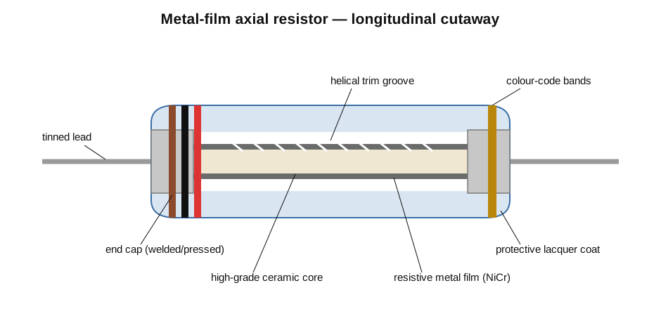
The rod is then trimmed exactly as the carbon-film part is — a helical groove ground through the metal film while the resistance is measured live — and finished with pressed-and-welded end caps, welded leads, and a lacquer coat. The construction is nearly identical to carbon film; the difference is entirely in the film material, and that difference is large. Metal film reaches 1% tolerance as an everyday grade (and 0.1% with care), holds a temperature coefficient of 50 or 25 ppm/°C and better, and generates far less excess noise because a continuous metal film has none of the granular carbon’s noisy micro-contacts. This combination — cheap axial format, tight tolerance, low tempco, low noise — is why the metal-film resistor became the modern general-purpose precision part, the small blue-or-beige-bodied 1% resistor that fills a modern through-hole board. The characteristic body color is only a coat pigment convention, but it has become a near-universal visual shorthand for “metal film, 1%.“

5.4 Metal-oxide film: hotter and flameproof
A close cousin trades some precision for heat and ruggedness. A metal-oxide film resistor deposits a film of a conductive metal oxide — classically tin oxide (SnO₂), often antimony-doped to set its conductivity — onto a ceramic rod, typically by spraying a tin compound onto the hot rod so it oxidizes in place rather than by vacuum sputtering. The oxide film is chemically stable, adheres tightly, and tolerates a higher operating temperature than a metal or carbon film can. Metal-oxide parts routinely run at surface temperatures where an ordinary film would degrade, carry more power in a given body size, and are commonly built as flameproof or fusible parts — coated so that an overload chars and opens the part safely rather than flaming. Their tempco and tolerance sit between carbon and good metal film — a few hundred ppm/°C and 2–5% are typical — so they are chosen for their thermal toughness, not their precision: mains-side dropping resistors, snubbers, inrush limiters, and anywhere a small axial part must shrug off heat and surges.
5.5 Thick film: the surface-mount chip in detail
The single most-made electronic component on Earth is the thick-film chip resistor, the tiny black rectangle produced by the trillion every year and scattered across the back of every phone, laptop, and appliance board. Understanding how it is built repays real attention, because almost everything about how a chip resistor behaves — its tolerance, its marking, its solderability, its failure modes — is a direct consequence of the process.
It begins with a large, thin substrate of alumina (aluminum oxide, Al₂O₃, typically 96% pure) — a stiff white ceramic tile, often several centimetres square, pre-scored on a grid into hundreds or thousands of tiny future chips. The substrate is an excellent electrical insulator and, importantly, a decent conductor of heat, which is how the finished chip sheds the power it dissipates into the circuit board beneath it. Onto this tile the maker screen-prints a resistive paste. The paste is a thixotropic ink whose active ingredient is ruthenium dioxide (RuO₂) — or a related ruthenate — suspended together with glass frit and an organic vehicle. A stencil screen defines exactly where each little resistor’s element lands, and a squeegee forces the paste through the open mesh onto the alumina. Print thickness is on the order of ten to a few tens of microns — hence “thick” film, in deliberate contrast to the sub-micron sputtered “thin” film below.
The printed tile is dried to drive off solvent, then fired in a belt furnace at around 850 °C. Firing burns away the organic vehicle and melts the glass frit, which flows and fuses the ruthenium-oxide grains into a solid, glassy composite bonded to the alumina. The finished resistive layer is a cermet — a ceramic-metal mixture — in which conduction happens through a percolating network of touching RuO₂ grains embedded in glass. That microstructure is exactly why thick film has the character it does: a moderate temperature coefficient (the industry standard is roughly ±100 to ±200 ppm/°C), a nontrivial voltage coefficient (the grain-boundary conduction is slightly field-dependent), and higher excess noise than a continuous metal film. It is not a precision material; it is a cheap, robust, screen-printable one, and its virtues are cost and manufacturability at colossal volume.
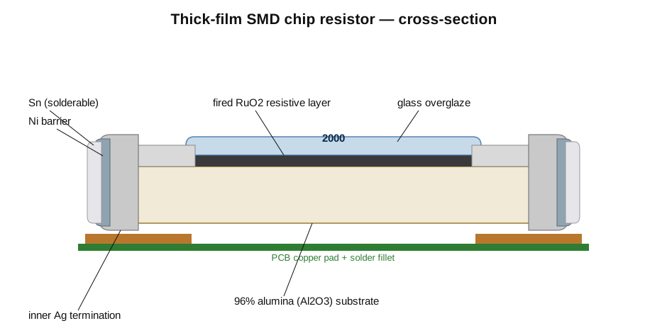
The terminations are where a chip resistor’s reliability is really engineered, and they are a small stack of layers, each with a job (Figure 3). The inner termination is a fired conductive paste — usually silver or silver-palladium — printed and fired at the element’s ends, wrapping over the edge so it contacts the resistive layer on the top face and provides a solid metal pad. Directly on the raw silver, though, solder would misbehave: molten tin-lead or tin solder dissolves silver greedily (silver leaching), so a bare silver termination can be eaten away during soldering. The fix is a nickel barrier layer, electroplated over the silver — nickel is nearly insoluble in solder and forms a wall the solder cannot cross, protecting the silver beneath. Finally, because nickel itself oxidizes and does not wet easily, an outer layer of matte tin (Sn) is plated over the nickel to give a fresh, readily solderable surface. The stack — fired silver inner, electroplated nickel barrier, tin outer, wrapped around each end — is why a chip resistor solders reliably and survives the reflow oven; it is worth knowing because a poorly made or old, oxidized termination is a classic cause of dry joints and open chips.
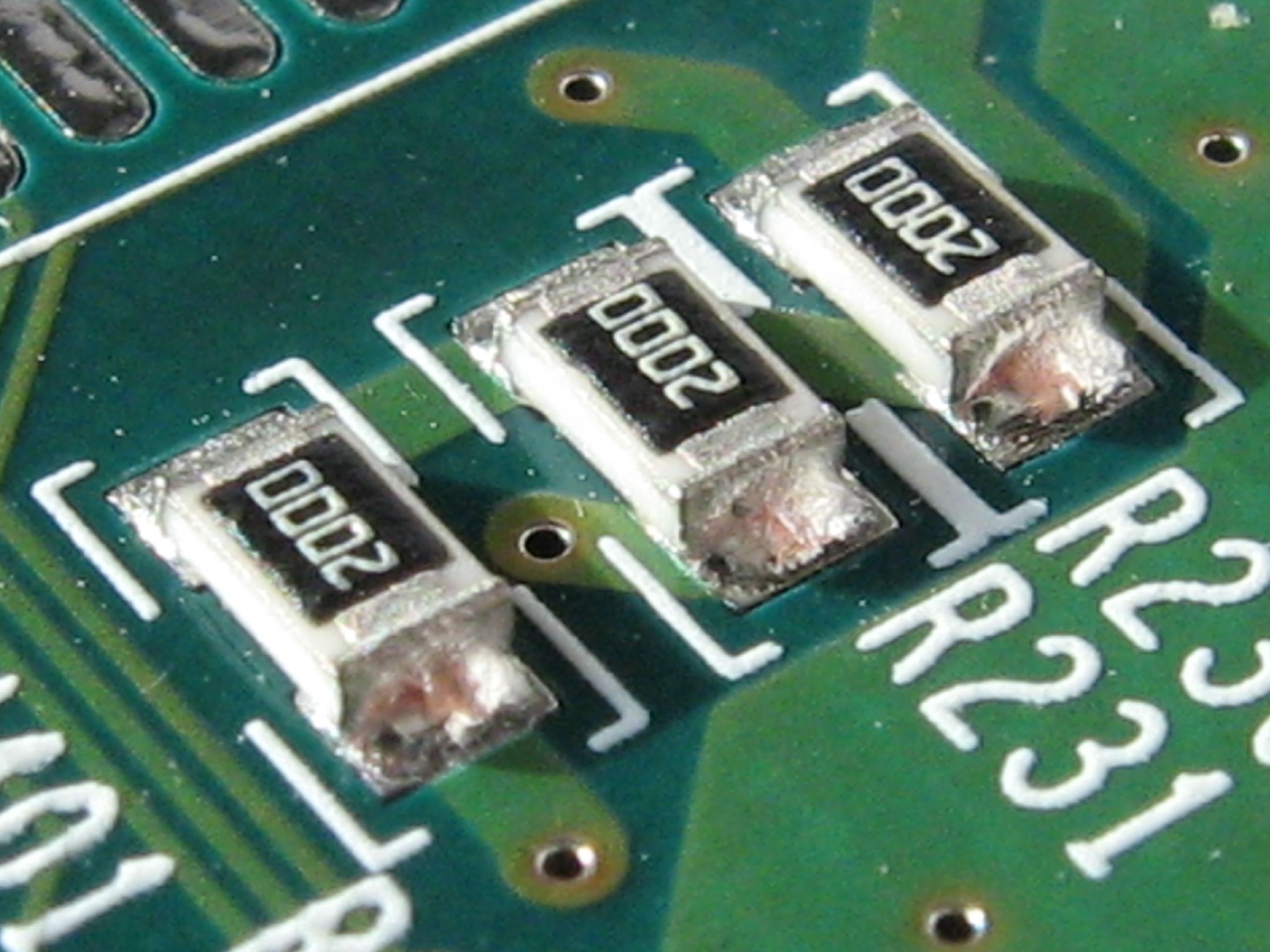
Between printing the element and the terminations, each individual resistor is laser-trimmed to value. Because thousands of resistors share one fired tile and the as-fired resistance scatters, a laser burns a small cut into each element while a probe measures its resistance live, raising the value to the target one chip at a time — the detail the trimming section returns to. After trimming, a glass overglaze (and often a second protective coat) is printed and fired over each element, sealing it against moisture and mechanical damage; this is the glassy black top surface of the finished chip. The maker then laser-scribes or snaps the substrate along its pre-scored grid, breaking the tile first into strips and then into individual chips, plating the exposed end faces as it goes so the terminations wrap fully around. A finished chip is finally marked — laser-etched or ink-printed with its value in the 3- or 4-digit EIA code, or with an EIA-96 code on the smaller sizes, or left blank on the tiniest bodies where no marking will fit. The marking convention itself — why “2000” means 200 Ω and not 2000 Ω, why “4R7” means 4.7 Ω — belongs to the reading-resistors volume; the point here is that the code is printed at the very end of a process that has already deposited, terminated, trimmed, glazed, and singulated the part.
5.6 Thin film: the precision chip
The chip resistor an instrumentation or precision-analog designer reaches for looks almost identical from across the bench but is made by a completely different, far more exacting route. A thin-film chip does not screen-print a paste; it sputters an ultra-thin, dense metal film onto the alumina substrate, then photolithographically patterns it — the vocabulary of semiconductor fabrication rather than screen printing. The film is typically nichrome (NiCr) or tantalum nitride (TaN), laid down only tens to a few hundred nanometres thick — a hundredth or less of a thick film’s thickness, hence “thin.” Instead of a stencil defining a blob of paste, a photoresist is spun over the whole sputtered film, exposed through a photomask, developed, and the film etched away everywhere except the precise resistor geometry the mask defined. The result is a continuous, homogeneous alloy film with an exactly defined shape rather than a grainy fired composite.
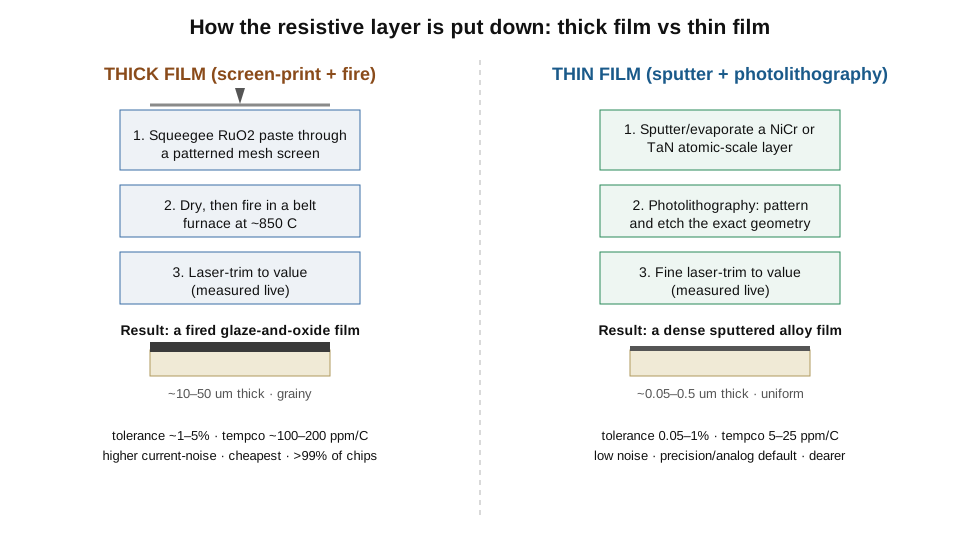
Everything that makes thin film the precision choice follows from that dense, continuous, thin, exactly-patterned film (Figure 5). Because the alloy is homogeneous rather than a percolating grain network, its temperature coefficient is low and repeatable — routinely 5 to 25 ppm/°C, an order of magnitude better than thick film — and it can be built with matched, opposing coefficients so that a whole network tracks temperature almost perfectly. Because the film is continuous, its excess noise is very low, approaching the thermal-noise floor, which matters enormously for low-level analog signal paths. And because photolithography defines the geometry to sub-micron accuracy and the film can then be laser-trimmed, tolerances of 0.1%, 0.05%, and tighter are ordinary. The price is literally a higher price: thin-film chips cost several times their thick-film equivalents, carry somewhat less power in a given size, and tolerate less energy in a surge. So the two technologies split the market cleanly — thick film for the trillions of ordinary pull-ups, biases, and dividers where 1% and 100 ppm/°C are plenty, thin film for the instrumentation amplifier’s gain network, the data converter’s reference divider, and anywhere the last few parts per million of stability earn their keep. The precision extremes of both, and how they compare with bulk foil, are the subject of the second fixed-types volume.
5.7 Wirewound: winding resistance wire on a core
Where a film must be thin and is therefore fragile against heat and surges, a wirewound resistor puts the resistance into a robust length of alloy wire, and in doing so reaches both the highest powers and — in a different guise — the highest precisions of any resistor family. The construction is exactly what the name says: a resistance wire is wound helically on a ceramic core, its ends welded to terminals or end caps, and the assembly coated to protect and, in power parts, to conduct heat away. The wire is not ordinary copper; it is a purpose-made resistance alloy chosen for the job. For power wirewounds the wire is usually a nickel-chromium alloy (nichrome) or a copper-nickel alloy, wound in a modest number of turns of relatively heavy wire to make a low-to-moderate resistance that can dissipate watts to tens of watts. For precision wirewounds the wire is a fine gauge of a special low-tempco alloy — manganin (copper-manganese-nickel) or Evanohm (a nickel-chromium alloy with additions) — wound in many turns, because these alloys can hold a temperature coefficient of a few ppm/°C and a stability that makes wirewound the traditional material of laboratory standard resistors and precision shunts.
The coating distinguishes the sub-types and is chosen for how much heat must escape. A molded or dipped cement/ceramic coating gives the familiar rectangular sand-colored power resistor. A vitreous enamel coating — a glass fired over the winding — protects higher-temperature parts and gives the classic green or grey cylindrical power resistor. A silicone coating suits parts that must tolerate high surface temperatures and some flexibility. And for the highest continuous power in the smallest package, the winding and its core are potted inside an aluminum housing — an extruded, often finned and anodized case — so that the resistor can be bolted to a chassis or heatsink and dump its heat by conduction rather than relying on still air. These aluminum-clad (also called aluminum-housed) power resistors are the workhorses of motor braking, power-supply loads, and dynamic braking banks.
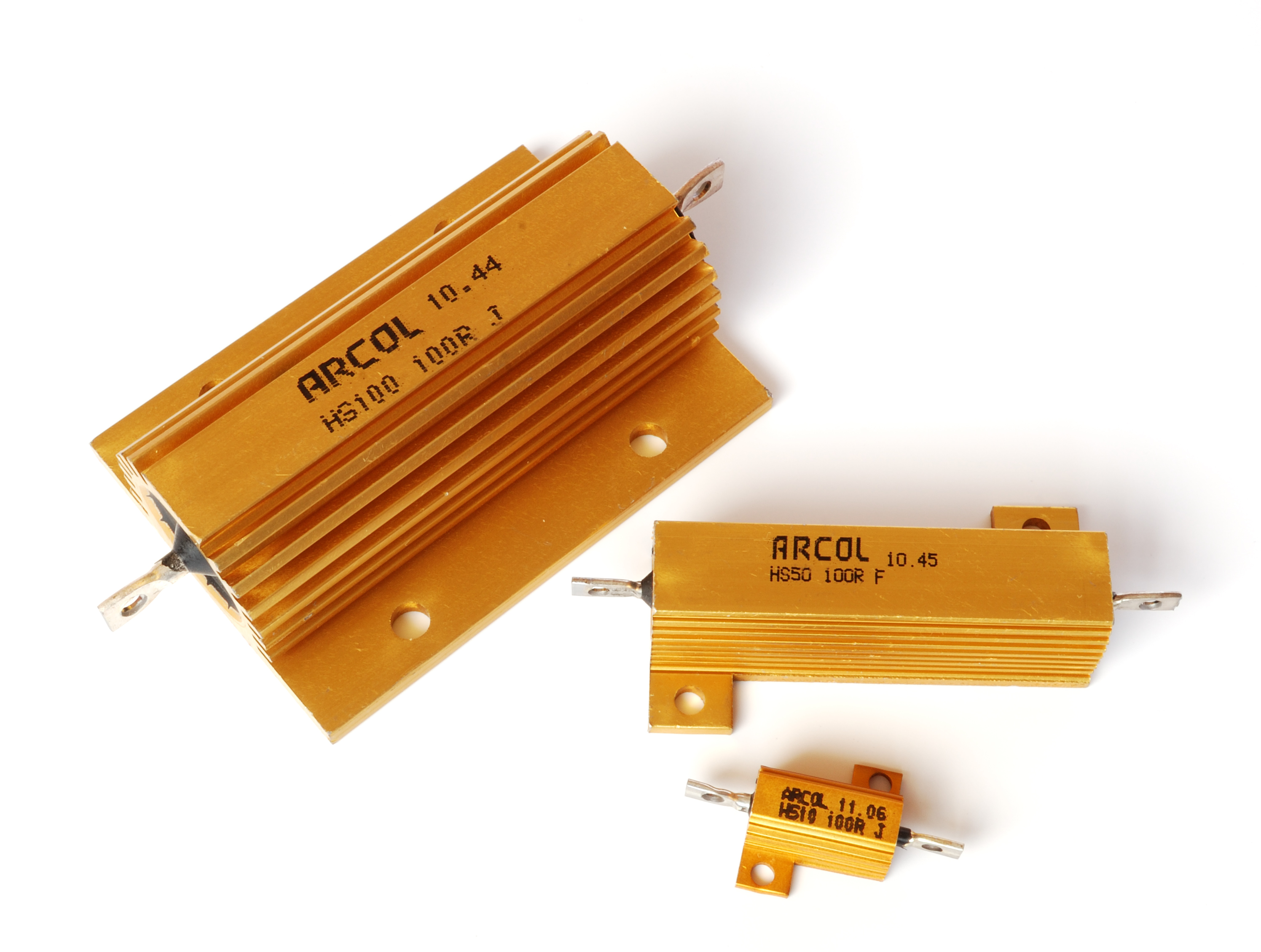
Wirewound’s one intrinsic drawback is written into its geometry: a coil of wire is an inductor. A resistor wound as a simple helix has a series inductance that makes its impedance climb with frequency, so a wirewound part that reads a clean value at DC can look quite different to a fast edge or an RF signal. Precision and high-frequency wirewounds are therefore wound non-inductively, most commonly by the Ayrton–Perry technique — two windings in opposite directions so their magnetic fields cancel — or by bifilar and reversed- sector windings that achieve the same cancellation. This matters enough, and interacts enough with the resistor’s parasitics, that the specialty-resistor volume treats non-inductive winding in its own right; the note here is simply that a wirewound resistor’s inductance is a consequence of how it is built and can be engineered away at some cost. Between them, heavy nichrome for power and fine manganin or Evanohm for precision, wirewounds occupy both ends of the resistor world that film cannot reach: the parts that must survive real power, and the parts that must not drift.
5.8 Bulk metal foil: the stability champion
At the very top of the stability ladder sits a construction that belongs to no other family: the bulk metal foil resistor, the reference-grade part chosen when nothing is allowed to drift. Its element is not deposited from vapor or fired from paste but cold-rolled from a nickel-chromium alloy into a thin foil — thicker than a sputtered film, a true piece of bulk metal — which is then bonded to a ceramic substrate and photo-etched into a fine serpentine pattern that sets the resistance. It reads a little like a thin-film chip built from a rolled foil instead of a sputtered layer, and the extra thickness of real metal is part of the point.
What makes bulk foil the stability champion is a clever piece of mechanical-electrical design. Every resistor’s value changes with temperature for two combined reasons: the alloy’s own resistivity changes, and the part physically expands, changing the element’s geometry. In a bulk-foil resistor the foil is bonded to a substrate whose thermal expansion is deliberately chosen so that, as temperature rises, the strain the substrate imposes on the foil changes the foil’s resistance in the opposite direction to the change in its intrinsic resistivity. The two effects are engineered to cancel, leaving a net temperature coefficient that can be held below 1 ppm/°C — better than the best wirewound and far beyond any film. The photo-etched foil element also has essentially no significant inductance or capacitance, very low noise, and excellent long-term stability and load-life. The cost is high and the power modest, so bulk foil is reserved for the places that justify it: metrology, precision references, strain-gauge and instrumentation front ends, and calibration standards. Its detailed performance and its rivalry with precision wirewound and thin film are drawn out in the second fixed-types volume.
5.9 Trimming: the unifying idea
Underneath all of these constructions runs one idea that deserves to be stated plainly, because it explains how a sloppy manufacturing process yields E96 tolerances at all. Every resistor is deposited or wound slightly too low and then trimmed up to value by removing material. You can only ever cut — never add — so the process starts below target and grinds, sandblasts, or burns material away while watching the value climb, stopping the instant it lands. There is no going back; overshoot the cut and the part is scrap. That asymmetry is why every trimming method is a closed loop: a four-wire ohmmeter reads the resistance continuously, a controller compares it to the target, and the cutting tool removes material only until the loop is satisfied (Figure 7).
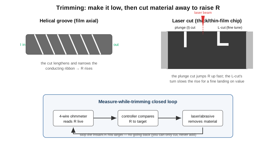
The methods differ by construction. On film axial parts the tool is a grinding wheel or diamond cutter that cuts the helical groove already described — the workhorse trim for carbon-, metal-, and metal-oxide-film rods, adjustable over a wide range by pitch and number of turns. Some parts, film and composition alike, are trimmed by abrasive or sandblast methods that erode the element’s cross-section. And the chip families are trimmed by laser, which is fast, precise, non-contact, and ideally suited to trimming thousands of tiny resistors on a shared substrate. Laser trimming has its own geometry vocabulary worth knowing. A simple plunge cut (also called an I-cut) drives straight into the element and raises the resistance quickly but coarsely — good for getting close in a hurry. An L-cut starts as a plunge and then turns ninety degrees to run parallel to the current flow; the turn sharply slows the rate at which further cutting changes the value, so the machine can creep the last fraction of a percent onto target without overshooting. More elaborate serpentine and double-cut geometries exist for the tightest tolerances. In every case the laser fires in short pulses while the probe reads the resistance between pulses, and the beam stops the moment the value is reached. This is how a fired paste that scatters ±20% as-printed becomes a ±1% part, and how a sputtered thin film becomes a ±0.05% one: not by depositing accurately, which is hopeless, but by depositing low and trimming up under closed-loop measurement.
5.10 Packaging and form factors
The same electrical element can be dressed in radically different packages, and the package — not the element — is usually what a board designer actually specifies. The oldest is the axial-leaded body: a cylindrical part with a wire lead emerging from each end, meant to pass through holes in a board and solder on the far side (through-hole mounting). Axial resistors are what most people picture when they hear “resistor,” they carry the color-code bands, and they remain the format for hand-built, prototyped, high-voltage, and higher-power through-hole work — but they have been displaced from mass production by the surface-mount chip.
The dominant modern package is the SMD chip — the flat thick- or thin-film rectangle that sits on top of the board and solders to pads on the surface, with no leads and no holes. Chips are named by a four-digit size code that encodes their footprint. The imperial code gives length and width in hundredths of an inch (mils): an “0805” is 0.08 by 0.05 inch. The metric code gives the same dimensions in hundredths of a millimetre: the same part is “2012,” meaning 2.0 by 1.2 mm. The two coding systems name the identical parts and are a perennial source of confusion, because “0603” imperial and “0603” metric are different sizes — the imperial 0603 is 1.6 × 0.8 mm, while the metric 0603 is 0.6 × 0.3 mm, which is the imperial 0201. The table and scale chart below give the standard family; unless a datasheet says otherwise, a bare size number quoted in English-language design practice is usually the imperial code.
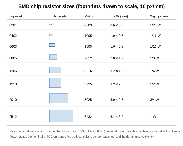
Table 1 — Packaging and form factors
| Imperial | Metric | L × W (mm) | Typical power |
|---|---|---|---|
| 0201 | 0603 | 0.6 × 0.3 | 1/20 W (0.05 W) |
| 0402 | 1005 | 1.0 × 0.5 | 1/16 W (0.063 W) |
| 0603 | 1608 | 1.6 × 0.8 | 1/10 W (0.10 W) |
| 0805 | 2012 | 2.0 × 1.25 | 1/8 W (0.125 W) |
| 1206 | 3216 | 3.2 × 1.6 | 1/4 W (0.25 W) |
| 1210 | 3225 | 3.2 × 2.5 | 1/2 W (0.5 W) |
| 2010 | 5025 | 5.0 × 2.5 | 3/4 W (0.75 W) |
| 2512 | 6432 | 6.4 × 3.2 | 1 W |
Dimensions per Vishay/Yageo thick-film chip datasheets; power ratings are nominal at 70 °C ambient on a specified land pattern and are vendor-dependent — always read the specific datasheet and its derating curve (see the power-and-derating volume).
Two things about the table are worth internalizing. First, the pattern of nominal dimensions is regular — the length and width step through a small set of standard values — which is why the size codes are memorable once the imperial/metric split is understood. Second, the power rating rises with body size for a simple physical reason: a bigger chip presents more area of alumina to conduct its heat into the copper of the board, so it can dissipate more before its element overheats. The ratings are nominal and assume a specified pad; a 2512 rated 1 W on a generous copper pour will be derated hard on a starved one, which is the whole subject of the derating volume. The very small sizes — 0402, 0201, and the sub-0201 metric parts — carry so little power and are so tiny that they are placed only by machine and often left unmarked.
A third SMD format bridges the axial and chip worlds: the MELF (Metal Electrode Leadless Face), a small cylindrical body with solderable metal end caps that sits in a saddle on the board rather than flat. A MELF is essentially an axial film resistor — usually metal film, with its helical trim groove — shrunk and given leadless end terminations instead of wire leads. Because its element is a helically-trimmed film on a round rod rather than a printed film on a flat chip, MELF parts offer better tolerance, tempco, pulse handling, and stability than a same-size thick-film chip, at the cost of a rounded body that is fussier to place and can roll. They survive in precision and pulse-tolerant surface-mount designs where the chip’s flat thick film is not good enough.
At the high-power end, resistors abandon the small-body formats entirely and adopt the packages of power semiconductors and the chassis. Power film and wirewound elements are built into TO-220 and TO-247 tabbed packages that bolt to a heatsink exactly as a power transistor does; into aluminum-housed (aluminum-clad) rectangular cases like those in Figure 6, bolted to a chassis; into open chassis-mount ceramic tubes with mounting brackets; and, for the highest power densities, onto insulated-metal-substrate (IMS) boards, where the resistive element sits on a thin dielectric over an aluminum baseplate that spreads and removes the heat. In every one of these the electrical element is one of the families already described; what changes is the thermal package, and the choice of package is really a choice of how the part will get rid of its heat — the theme the power volume develops in full. The marking of all these parts — the color bands on axial bodies, the printed 3-/4-digit and EIA-96 codes on chips, the plain printed value-and-tolerance on power cases — is its own small language, and reading it fluently is the entire job of the next volume.
5.11 From construction to specification
Every specification a later volume quotes is, at bottom, a fingerprint of the construction described here. A resistor’s tolerance is set by how finely it was trimmed and how stably its element holds that value — a helically ground carbon film lands at 5%, a laser-trimmed thick-film chip at 1%, a photolithographic thin film at 0.05%, a bonded-foil element below that. Its temperature coefficient is a property of the element material and, in bulk foil, of a deliberate strain-cancellation trick — hundreds of ppm/°C for carbon and thick film, tens for metal and thin film, single digits for precision wirewound, below one for foil. Its noise tracks the same divide: granular carbon and cermet films are noisy, continuous metal and foil films are quiet. Its power rating is a thermal property of the package — the body size, the coating, and how well the whole assembly conducts heat away. And its parasitic inductance is a consequence of geometry, worst in a plainly wound wirewound and engineered away by Ayrton–Perry winding or a non-inductive layout. The power-and-derating volume takes up the thermal side, the fixed-types volumes take up the material-by-material character sketches, and the specialty volume takes up the non-inductive and sensing constructions — but each of them is reading, in the language of specs, the same four-step story this volume told in the language of the factory: deposit or wind the element, connect it, protect it, and trim it to value.
Comments (0)